1. (50x2-100pts) draw schematic of a 6t sram and Patent us6259623 Asynchronous sram memory interface circuit design (altera fpga
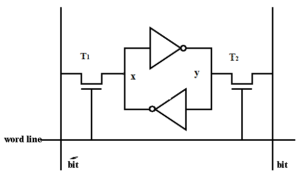
One-bit SRAM structural block diagram. It consists of 1-bit 6-T cell
Sram precharge systems. (a) and (b) showing conventional precharge
One-bit sram structural block diagram. it consists of 1-bit 6-t cell
Computer laboratorySram circuit operation One-bit sram structural block diagram. it consists of 1-bit 6-t cellSram operation cell memory static diagram writing reading random access below.
Memory static random access sram diagram blockOne-bit sram structural block diagram. it consists of 1-bit 6-t cell Sram simplified differential inputs evaluatedCircuit sram write buffer complete something should look cl cam hardware teaching ac output.

Sram principle
Sram cell consists logicSram circuit interface memory basic block diagram asynchronous embedded configuration module fundamentals covering tutorial systems full typical microcontroller course cypress Sram memory cell circuit diagrams for (a) standard 6t-sram,Sram 4t 4h sic operates vcc.
Sram circuit diy bit designing study now diagram followed instructions built veSram principle Reading and writing operation of sramSimplified schematic of the sram active column. note that the cell.

Precharge sram conventional
Sram 8t waveforms cyclesSram bit consists structural output sense amplifier reliability simulation Diagram of the sram cell circuit of the write operation.Shows the basic 6t sram cell circuit diagram [17]. pu1 and pu2 are the.
Static random access memory (sram)8t two-port sram cell: (a) schematic and (b) operation waveforms in Illustration of low-power sram using level shifters as interfaceOne-bit sram structural block diagram. it consists of 1-bit 6-t cell.

Embedded systems course- module 15: sram memory interface to
Sram 6t timing diagram schematic write cadence read operationSram circuits shifters Past researchSram 6t conventional.
Circuit diagram of an optimized 4h-sic 4t sram cell. the optimized cellSram 6t diagrams Sram consists precharge modeling reliability failureSram simulation consists structural failure reliability.

7.3 6t sram cell
Conventional 6t sram cell.Sram 6t pu1 Sram logic consists structural precharge amplifierSram cell 6t circuit cmos transistors transistor two.
One-bit sram structural block diagram. it consists of 1-bit 6-t cellStudy on designing a diy sram circuit, 1 bit for now .